

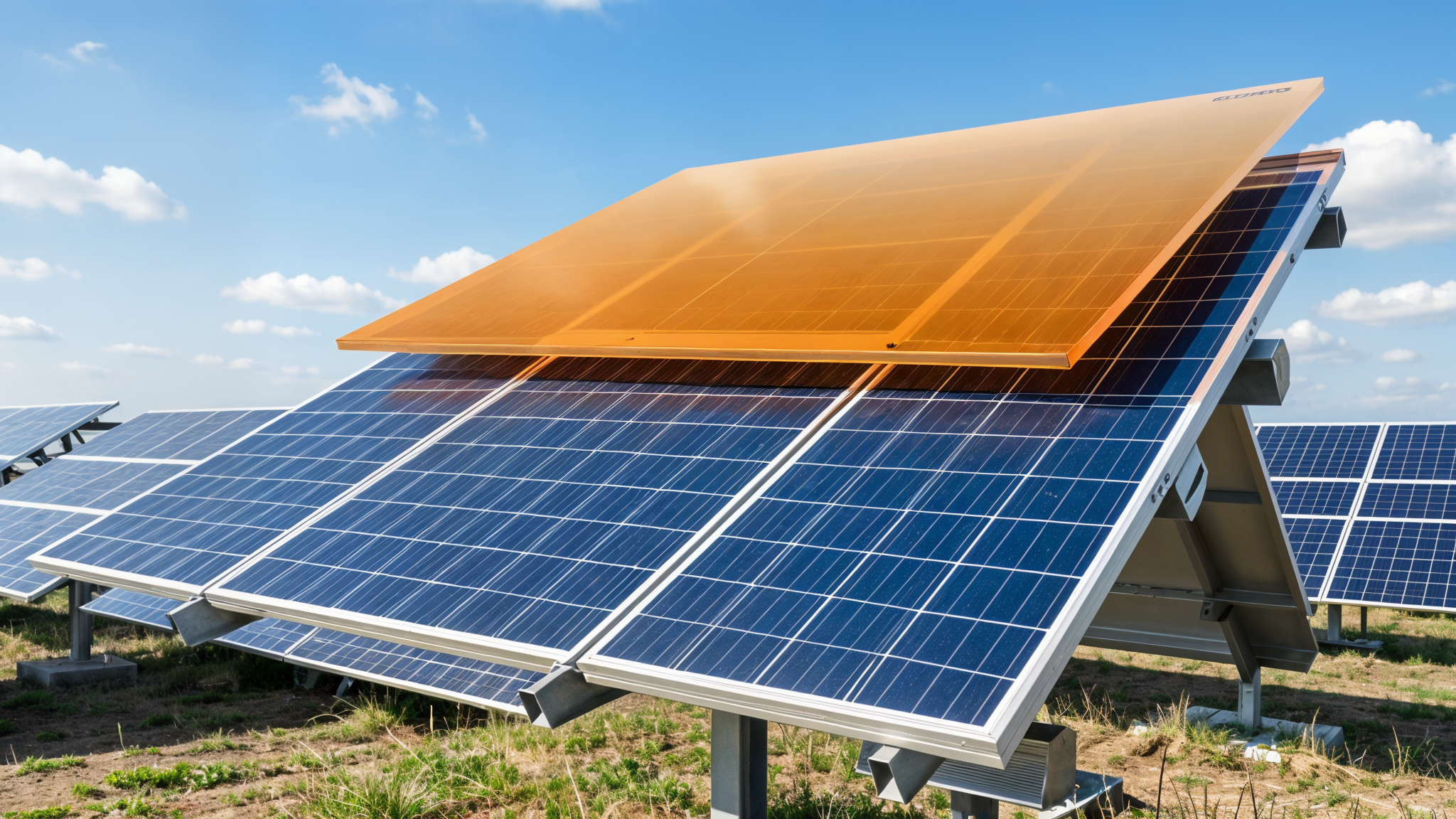
We have been hearing for decades that solar energy is going to change everything. And it has: panels on rooftops are now a common sight, prices have plunged 90% since 2010, and in many countries photovoltaics is the cheapest way to generate electricity. But the dominant technology —silicon— has a physical ceiling. Its maximum theoretical efficiency is around 29%, and in practice commercial modules land between 22% and 24%. That is where perovskite comes in.
In recent months, laboratories have strung together efficiency records at an almost weekly pace. Tandem cells —a layer of perovskite on top of a layer of silicon— have already surpassed 34% certified efficiency. That means that, with the same surface area, a third more electricity is generated. It is not a distant promise: companies such as Oxford PV (UK), Swift Solar (USA) or CubicPV (USA) have already started pilot production, and the first large-scale commercial deliveries are planned for 2025-2026.
What exactly is perovskite?
The name comes from a crystalline structure discovered in the Urals in 1839, but what researchers use today is a family of synthetic materials —organic-inorganic metal halides— that can be deposited in a thin layer at low temperature, almost as if it were ink. Unlike silicon, which requires furnaces above 1,000 °C and ultra-pure ingots, perovskite is printed roll-to-roll, on flexible substrates or directly on top of a finished silicon cell.
That ease of manufacturing opens the door to lighter, flexible panels that are, in theory, much cheaper. But the great asset is optical: perovskite absorbs the blue and green light of the spectrum, while silicon keeps the red and infrared. Together they cover much more of the spectrum than each one separately. Hence the jump in efficiency.
The great obstacle: stability
For years, perovskite was a laboratory star that degraded within weeks when exposed to humidity, heat or continuous light. That has changed. The best current formulations —encapsulated with advanced glass and polymer barriers— already pass accelerated aging tests equivalent to 25-30 years outdoors. Oxford PV, for example, certifies that its tandem modules retain 92% of their power after 1,000 hours of extreme humidity and heat (IEC 61215 test), and projects annual degradation of under 0.5%, comparable to silicon.
The key has been interface engineering: more robust charge transport layers, additives that curb ionic migration, and airtight encapsulates that block water vapor. There is still no single standard —each company has its own recipe— but the convergence toward stable materials is real.
When will we see them on rooftops?
Oxford PV has already shipped its first commercial modules to a customer in the USA (a pilot installation of 72 cells, 580 W per panel). Swift Solar has demonstrated lightweight flexible modules for mobile and aerospace applications. CubicPV is betting on a hybrid approach: thin silicon wafers with perovskite printed on top, manufactured on a continuous line that promises per-watt costs well below current ones.
The common roadmap is clear: 2025-2026 for pilot projects and high-value niches (roofs with weight restrictions, vehicles, satellites), 2027-2028 for entry into the mass residential and commercial market. Silicon is not going to disappear —its supply chain is massive and mature— but tandem perovskite is shaping up as the natural successor to squeeze out more watts per square meter.
What it means for the energy transition
More efficiency means less land, less steel, less glass and less labor per installed megawatt. In a world that needs to triple installed solar capacity by 2030 according to the IEA, every percentage point counts. Tandem perovskite can reduce the levelized cost of electricity (LCOE) of solar by a further 15-20% compared with cutting-edge silicon, according to models from NREL and Fraunhofer ISE.
In addition, its low-temperature manufacturing fits with industrial decarbonization: it can be integrated into existing factories without silicon’s massive furnaces, and its manufacturing carbon footprint is potentially smaller. If the supply chain scales up —chemical precursors, deposition equipment, encapsulates— perovskite can become the second great driver of cheaper solar after silicon’s learning curve.
Challenges remain: scaling production without losing performance, standardizing reliability tests, managing the lead (present in the most efficient formulations, although in minimal and encapsulated quantities) and proving bankability so that financiers accept the technological risk. But science has already done its part. Now it is the turn of industrial engineering. And that, unlike physics, has no theoretical ceiling.