

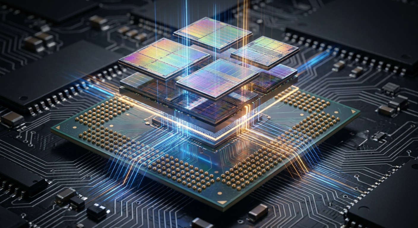
For half a century a chip was one piece: a silicon wafer, a square die, a package and pins. Everything the processor did lived inside that die, built in a single pass with the same process. That idea is breaking down. The most advanced chip on sale today is not a monolithic die but an assembly of several dies —chiplets— joined inside the same package, sometimes stacked vertically, and connected by interfaces that until recently existed only between separate circuit boards.
The reason is not aesthetics. It is manufacturing arithmetic.
The reticle rules
An extreme-ultraviolet lithography scanner prints a chip pattern with a maximum field of roughly 26 by 33 millimetres: the mask reticle. That is about 858 mm² of usable area per exposure. A larger die requires stitching several exposures together, which complicates the technique and balloons the cost.
But the decisive argument is manufacturing yield. Defects on a wafer are distributed roughly at random, so the probability that a die comes out clean falls exponentially with its area: the Poisson model estimates it as Y = e−D·A, where D is the defect density per unit area and A the die area. Going from 800 to 200 mm² does not just quadruple the number of chips per wafer: it also shrinks the fraction that gets thrown away. A small defective die costs little; a large defective die is discarded whole after dozens of expensive steps.
There is a second, subtler reason: not everything shrinks the same way. Digital logic advances with each node, but SRAM barely gains density and the analogue input/output circuitry (memory PHYs, high-speed links) stalls for generations. Building the entire chip on the most expensive node so that half the area is I/O that does not benefit from it is a waste of money. The answer is to split: logic on the leading node, cache on an intermediate one, I/O on a mature, cheap one, and join the pieces afterwards.
What a chiplet actually is
A chiplet is an independent functional die —a CPU core, a GPU matrix, an accelerator, a memory controller, an Ethernet PHY— built on whichever node suits it best and tested on its own. The package stops being passive protection and becomes the interconnect system. You gain yield, reuse (the same I/O die serves several generations and several products) and time to market. You pay in complexity: you have to design the die-to-die interface, coordinate their boot and make sure the whole behaves as a single device.
From gold wire to solderless copper
Die-to-die connection has gone through several generations. Classic wire bonding links the die’s contacts to the substrate with gold or aluminium wires; it works, but only around the perimeter and with tens of micrometres of pitch. Flip-chip turned the die over and connected it with thousands of tiny tin spheres spread across its whole face. The next leap was the interposer: an intermediate silicon wafer, pierced with vertical vias (TSVs) that go right through it, acting as a copper bridge between dies with pitches of tens of micrometres. That is the basis of the CoWoS processes, able to host interposers up to about 3.3 reticles in area, roughly 2,700 mm².
The alternative without a full interposer is bridges embedded in the substrate, which connect only the dies that need it. And at the density extreme sits hybrid bonding: the silicon dioxide and copper surfaces are polished flat and brought into direct contact, with no solder, so the copper pads diffuse into each other. Pitch drops from the initial 40 µm to around 9 µm, with a roadmap heading towards 3 µm. Less pitch means more connections per millimetre of edge, less parasitic capacitance and less energy per bit. This is the technique that lets twelve layers of HBM memory be stacked on one package and push past a terabyte per second per stack.
UCIe: the protocol that brings order
For years every vendor invented its own interface. In 2022 several major players agreed on an open standard, UCIe (Universal Chiplet Interconnect Express), so that dies from different companies could coexist in one package. UCIe defines three layers. The physical layer sets the bump pitch —45 µm in the standard variant, 25 µm in the advanced one—, the data lanes, the forwarded clock, a sideband channel to exchange parameters and spare lanes to repair faulty connections. Per-lane speed started at 4-32 GT/s, and the most recent revision raises it to 48 and 64 GT/s.
Above it sits the die-to-die adapter: it packs data into 68-byte flits for PCIe and CXL or 256-byte flits for streaming, adds CRC and retransmission, and handles link training. And on top, the protocol layer, which can present itself as PCIe, as coherent CXL or as a proprietary streaming link. The metric that matters is not absolute bandwidth but density: on the order of 224 GB/s per millimetre of edge with 32 lanes at 32 GT/s, and 3.24 times more at 25 µm pitch. Energy is around 0.5 pJ/bit in the standard variant and 0.25 pJ/bit in the advanced one, against the tens of pJ/bit it costs to carry the same signal across the board with a conventional SerDes.
What breaks along the way
The first problem is testing. Before joining dies you have to know which ones work: the known good die. A single faulty die ruins a package worth thousands of euros that can no longer be taken apart, so dies are tested on the wafer and repair lanes are added to the link. The second is thermal. Power per square millimetre piles up, and a stack of HBM glued to the logic heats them both; silicon and the organic substrate have different expansion coefficients and the package warps. The third is power delivery: feeding current to tens of billions of transistors through ever finer traces causes voltage droop. The answer is backside power delivery: moving the power network below the transistor plane with nano-TSVs, as Intel does with PowerVia on its 18A node, frees the front-side traces for signals and cuts resistive droop.
And there is a fourth front almost nobody watches: security. The interposer is a shared physical bus between dies; if one die cannot be trusted, it can snoop on or tamper with its neighbours’ traffic. UCIe provides for link integrity and confidentiality, but that adds latency and burns energy. Software, too, has to assume the assembly is a single coherent device, with distributed caches and firmware that trains the links at boot.
The consequence of all this is a shift in where the race is won. For decades it was measured in transistors per square millimetre. Now it is also measured in square millimetres of interposer, in watts per bit and in degrees per watt. The next leap is not only in the transistor: it is in how the pieces are glued together.