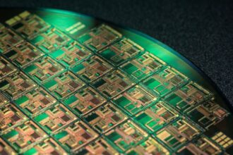


Silicon has spent almost seventy years being the material from which virtually all of the world’s solar electricity is made. It is abundant, it stays stable for decades and the industry has learned to produce it in wafers measured in square metres at a ridiculous cost. But it has a clear physical ceiling: a single-junction silicon cell cannot convert more than roughly 33.7 % of the energy in light into electricity, and real panels on real roofs sit closer to 23-24 %. The way out is not to abandon it but to put another cell on top of it. In July 2026, LONGi announced a silicon-perovskite tandem cell certified at 35.5 % by the European institute ESTI: a figure that, for the first time, comfortably beats the limit of a single cell.
Why two materials convert more than one
A solar cell works with a semiconductor that has a bandgap: the minimum energy a photon needs to knock an electron loose and send it around a circuit. In silicon that energy is 1.12 electronvolts, which corresponds to photons in the deep red and near infrared. Higher-energy photons — blue and violet — are absorbed too, but the electron they release drops straight to the band edge and the surplus energy is lost as heat, a process called thermalisation. And photons with less energy than the bandgap simply pass through the cell without doing anything.
That double waste is what the Shockley-Queisser limit quantifies: with a single bandgap, part of the spectrum is always thrown away. The answer is to split the work. A perovskite cell with a wide bandgap, around 1.6-1.7 eV, absorbs the high-energy photons first; whatever it does not absorb passes through and reaches the silicon, which takes the red and the infrared. Each layer works with the slice of the spectrum that suits it best, and the complete tandem can beat the ceiling of a simple cell. The theoretical limit for a two-junction silicon-perovskite tandem sits around 43 %; for an all-perovskite tandem, close to 47 %.
What a perovskite actually is
The name does not describe one material but a family of crystals sharing a common structure: ABX3. The A site usually holds an organic cation or caesium (formamidinium, methylammonium), the B site a metal — normally lead, in some variants tin — and the X site a halide, iodide or bromide. The crystal lattice is a framework of corner-sharing octahedra that tolerates swapping the pieces: by mixing bromide and iodide in different proportions and adjusting the A-site composition, the bandgap can be moved at will between roughly 1.5 and 2.3 eV. That tuning is exactly what silicon cannot do, because its bandgap is fixed by the physics of the material.
The second attraction is how it is made. A perovskite is not grown in a furnace at 1,400 degrees like crystalline silicon: it is deposited as an ink — precursors dissolved in an organic solvent — spread over the substrate and crystallised with a heat treatment of barely 100-150 degrees. The active film is about 500 nanometres thick, a thousand times thinner than a silicon wafer, and the coating techniques come from the printing and glass industries: slot-die, capillary meniscus, printing. Cheap material and a fast process, in theory.
Two cells in series: the current knot
The architecture industry is chasing is the two-terminal one: the perovskite cell is deposited directly onto the silicon cell and the two are wired in series, with an intermediate layer — the recombination junction, which behaves like a tunnel junction — letting charge move from one to the other without losing voltage. The result is a single cell with two contacts, easy to drop into a conventional panel.
That stack imposes a hard constraint: because the two cells are in series, the current the pair produces is the current of whichever layer produces less. This is the photogenerated current of the limiting junction. If the perovskite absorbs too much, it leaves the silicon without photons and half the spectrum is lost; if it absorbs too little, the top layer becomes the bottleneck. So the thickness and bandgap of the upper absorber are calculated to the millimetre, and not for peak efficiency under laboratory conditions but for the best energy yield across a whole day, with the sun changing angle and colour. Alternatives exist — the four-terminal layout, with two stacked cells on independent circuits, easier to optimise and considerably more expensive to build — but the industrial route is two-terminal.
The texture problem
Here the first serious manufacturing difficulty shows up. A modern silicon wafer is not flat: its surface is etched with microscopic pyramids that trap light by bouncing it several times inside the material. The contacts are selective — TOPCon or amorphous-silicon heterojunction — and the whole process is tuned to that micrometre-scale roughness. A perovskite top cell has to adapt to that surface: it must be deposited conformally, covering the apexes and the faces of every pyramid with an even thickness, with no pores and no thinned patches.
No single technique solves it alone. The hybrid route combines part of the film deposited in vacuum (evaporation or chemical deposition) with another part from solution, or uses blade coating over the texture, and then adds the transparent top contact — conductive oxides such as ITO or IZO — and the recombination junction, all without damaging the layers underneath. On a flat wafer, laboratory performance is excellent; the challenge is carrying those numbers over to textured wafers at industrial format, on the order of 260-280 square centimetres. LONGi reported 34.3 % on 261 cm² and 32.2 % on 274 cm² in 2026, against the 35.5 % absolute record on a small area. That three-point difference is, to a large extent, the price of texture and scale.
Stability: the real enemy
A perovskite is a soft, mobile crystal. Its ions, especially the halides, move inside the lattice when there is light, heat or an applied electric field. The best-known effect is halide segregation: in iodide-bromide mixtures, sustained illumination makes the bromide-rich phase cluster into domains, the bandgap drifts out of tune and the open-circuit voltage drops. On top of that come sensitivity to moisture and oxygen, thermal degradation above roughly 85 degrees and corrosion of the metal electrodes, which can accelerate ion migration.
To sell a panel you have to pass IEC 61215, which includes damp-heat tests at 85 degrees and 85 % relative humidity for a thousand hours, thermal cycling between -40 and +85 degrees, humidity freeze, plus partial-shading and reverse-bias tests. Laboratory devices that survive under continuous illumination are measured with ISOS protocols and, in the best case, the time to lose 20 % of performance is around a thousand hours. In the sector, one of the most quoted data points is Hanwha Q CELLS’ 95 % retention after 1,000 hours of maximum-power-point tracking. The first tandem modules with full industrial certification already exist and some commercial prototypes push those damp-heat and cycling sequences to three times the standard, but the margin against a silicon panel’s 25-year warranty is still the open question.
Who is close to selling it
The laboratory and the factory are in different places. The record belongs to LONGi, which over the past three years has gone from 33.9 % to 34.6 %, to the 35.2 % listed in Martin Green’s efficiency tables, and finally to the 35.5 % certified by ESTI in July 2026. On small areas, KAUST has been moving around 33 % and other manufacturers such as Q CELLS sit near 31-32 %.
The company closest to production is Oxford PV, with a commercial line in Brandenburg, Germany, and a 60-cell residential module certified by Fraunhofer CalLab at 26.9 % — far below the cell record but already a product. In the United States, Caelux and Tandem PV run pilot lines of tens of megawatts a year dedicated to tandem modules in commercial format. Scale is still measured in megawatts, while single-junction perovskite is already being produced in China at gigawatt scale; the tandem depends on the silicon industry rather than replacing it, so its rollout will consist of adding deposition steps to lines that already exist.
What still has to be solved
Three fronts remain. The first is lead: the absorbing layer contains it, and although the amount per square metre is small and it sits inside an encapsulant, a broken panel on a roof exposed to rain is an emission pathway, and perovskite is water-soluble. Hence the research into lead-free alternatives (using tin, which oxidises easily) and into encapsulants that trap any leakage is as active as the work on efficiency. The second is the jump from cell to module: records are measured in square centimetres, and the losses of cell interconnection, glass or a transparent contact with the right sheet resistance eat several percentage points. The third is recycling and the full lifecycle cost, which will only be known once production moves from thousands to millions of square metres.
The technological conclusion is awkward for anyone expecting a replacement: perovskite is not coming to retire silicon, it is coming to lean on it. In a tandem, silicon still does half the work and still supplies the two things perovskite does not yet have: demonstrated stability and a mature production chain. Those certified 35.5 % are not a new cell; they are an old cell pushed past its own limit.