

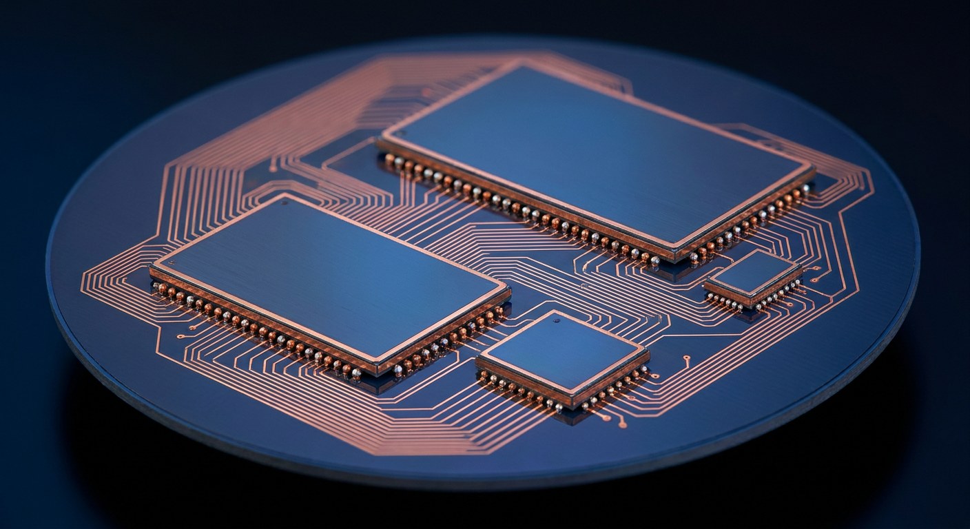
A high-end processor is no longer a single piece of silicon. A few years ago, manufacturers stopped trying to fit everything into one die — the slice of wafer already cut and ready to be packaged — and began splitting the work across several. The reason is not fashion: it has to do with the physics of lithography, the mathematics of manufacturing yield and the real cost of every square millimetre of silicon.
The limit nobody can cross
Extreme ultraviolet (EUV) lithography scanners print a field of at most about 26 × 33 millimetres. That rectangle is called the reticle limit, and it is not a commercial decision: it comes from the size of the mask that the light projects onto the wafer. A large monolithic chip, like the ones made a decade ago, was already brushing against that ceiling. Growing beyond it left two options: shrink the transistors — increasingly expensive and leakier — or split the design into several dies that talk to each other inside the same package.
The second option is the one that won. That family of designs is called chiplets: instead of one monolithic processor, several smaller dies, each built in the node that suits it best. Compute cores in an advanced node, cache in a more mature and cheaper one, input/output controllers in another. Nobody wastes wafer area building 3-nanometre logic for a function that does not need it.
Why splitting the chip saves money
The economic argument is manufacturing yield. Defects on a wafer are distributed roughly at random, and the Poisson model says the probability that a die comes out good falls exponentially with its area. Doubling a die’s area does not double the cost: it multiplies it. If area grows fourfold and yield per wafer drops from 80% to 40%, every good chip costs four times as much as before. With small dies, far less wafer is thrown away and each part can be tested separately before assembly: this is what the industry calls known good die, verified parts that do not ruin the whole when one of them fails.
How two neighbouring dies talk
The technical challenge is not cutting: it is joining back together. Two dies in the same package must exchange data with latency and bandwidth comparable to those of an internal bus. That is what die-to-die interconnects such as UCIe (Universal Chiplet Interconnect Express) are for: an open standard defining the physical layer, the protocol and the power management of the link. UCIe reuses ideas from PCI Express, but over millimetre distances and with much faster clocks: we are talking tens of gigabytes per second per millimetre of die edge, at a few picowatts per bit.
Physically, the dies rest on an interposer: an intermediate silicon wafer with microscopic traces linking one die to another. In 3D designs, TSVs (through-silicon vias) are drilled vertically through the die itself to stack layers of memory or compute. Each of those contacts is closed with solder microspheres, the bumps, tens of micrometres across. An advanced package can hold hundreds of thousands of these joints, and a single cold bump ruins the link.
The problem few people mention: heat
Splitting the chip does not split the heat. Quite the opposite: it concentrates power density in small areas and forces dozens of watts per square centimetre to be removed through several layers of materials with different thermal expansion coefficients. When the silicon expands more than the substrate, the joint cracks. That is why modern packages include thermal interface materials, metal lids and, in the most aggressive designs, liquid-cooling microchannels built into the interposer. Temperature does not only cap frequency: it also shortens the life of the bumps and the TSVs.
Who is using this architecture
AMD was the first to take chiplets to large scale with its EPYC processors, separating the cores (CCD) from the input/output hub (IOD) and linking them through Infinity Fabric. Intel has followed a similar path with disaggregated designs and its EMIB technology, which replaces the full interposer with small silicon bridges embedded in the substrate. Apple, with its M-series chips, stacks high-bandwidth memory next to the compute die; and AI accelerators in large data centres have turned 2.5D packaging into the real production bottleneck: lithography is not in short supply, interposers and assembly capacity are.
The next step is already in the labs: standardising the package so that a die from one vendor can live alongside another’s. UCIe aims at exactly that, just as PCIe allowed cards of any brand to be mixed. If the standard takes hold, a customer will be able to combine cores from one company with memory from another and accelerators from a third on the same interposer. That is the real change: the chip stops being a closed product and becomes a catalogue of parts.
What this means for the user
In the short term, nothing visible: programs keep working the same way. In the medium term, plenty. Chiplets let the same compute die be reused in laptops, servers and consoles by changing only the surrounding parts, which cheapens development and speeds up new versions. They also make it possible to repair — or at least replace — parts of the package without discarding the whole. And they explain why memory and advanced-packaging prices have become so sensitive: assembly capacity is now as critical as the ability to print transistors.