
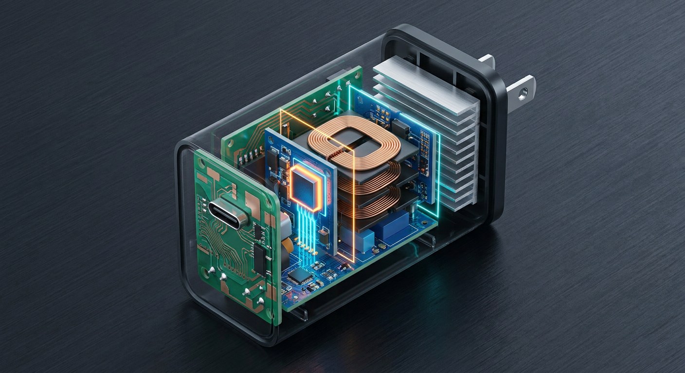
In 2010, a 65-watt laptop charger weighed 300 grams, took up half a backpack pocket and got hot enough that you did not leave it on the living-room table. Today the same watts come out of a 60-gram cube you plug straight into the wall. It is not that we learned to make thinner copper: the switch inside has changed, and with it the entire arithmetic of the power supply.
Why silicon hit its ceiling
A switched-mode supply does not regulate voltage with resistors. It turns a transistor on and off tens or hundreds of thousands of times per second and lets the inductor and the output capacitor turn that pulse train into a stable direct current. The transistor therefore spends its life in two states that ideally dissipate nothing: closed (zero voltage) or open (zero current). The problem is the transition.
In a silicon MOSFET, holding off 650 volts requires a lightly doped drift region about 50 microns thick. That region is, literally, a series resistance with the load: the thicker it must be to withstand voltage, the higher its on-resistance. The figure of merit designers use, the Baliga FOM (proportional to mobility times the cube of the critical breakdown field), sums up the trade-off: with silicon, whose critical field is 0.3 MV/cm, the resistance-area product is high and the die has to be large. A large die brings more gate capacitance and more stored charge, which forces a beefier driver and slower transitions.
Losses split into three accounts: conduction (I²·RDS(on) times duty cycle), switching (½·V·I·(tr+tf)·f) and gate drive (Qg·Vgs·f). The last two grow linearly with frequency. With silicon, going from 65 to 300 kHz to shrink the transformer costs too much heat, which is why the 2010 bricks stayed at tens of kHz and huge ferrite cores.
What gallium nitride changes
GaN has a bandgap of 3.4 eV against 1.1 eV for silicon and a critical breakdown field of around 3.3 MV/cm, ten times higher. That allows a drift region ten times thinner and far more heavily doped: resistance per unit area drops by two orders of magnitude in theory and by ten to twenty times in commercial devices. For the same voltage, the switch can be much smaller, with less gate charge and faster transitions.
The device is not a conventional MOSFET but a HEMT (high-electron-mobility transistor). An AlGaN layer is grown over GaN; the polarisation difference between the two creates a sheet of free electrons at the interface, the 2DEG, with no need for dopant impurities. Without impurities to scatter them, electrons keep a mobility of 1,500-2,000 cm²/V·s and the sheet conducts with a very high charge density. The historical catch is that the channel exists even when you do not ask for it: the classic HEMT is depletion-mode, normally on. Designers solve it with a p-GaN gate that depletes the 2DEG at rest (enhancement mode) or with a cascode arrangement using a low-voltage silicon MOSFET.
Two details separate GaN from silicon and power-supply engineers know them well. It has no body diode: in reverse conduction it conducts through the 2DEG itself, with a higher voltage drop, so the dead time between the two switches of a half bridge has to be tuned precisely or you get losses and parasitic turn-on. And it has no comparable avalanche capability: there is no UIS curve guaranteeing it survives an overvoltage, so the design is done with margin and clamps rather than trusting the device to limit itself.
More frequency, a smaller transformer
Faraday’s law says voltage per turn is proportional to core area and to the rate of change of flux. Multiply frequency by four and the core can have a quarter of the area for the same turns-to-power product. That is where the slimming of the charger comes from: not the transistor, but the transformer that no longer has to be big. A 65 W GaN charger typically runs between 200 and 500 kHz, using active-clamp flyback topologies at medium power and resonant half-bridge LLC designs above 100 W.
As frequency rises, the transformer becomes planar, with windings printed on the board itself and a controlled air gap; the secondary rectifier becomes synchronous, another MOSFET instead of a Schottky diode, and control moves to a digital integrated circuit that speaks USB Power Delivery. In version 3.1 the standard allows up to 48 V and 240 W, and PPS mode adjusts voltage in 20 mV steps so the phone asks for exactly what its battery needs at each stage of charging. That feedback loop, in many designs without an optocoupler, is closed by measuring the primary voltage during dead time.
The hidden price: heat and electromagnetic noise
Packing 65 W into 70 cubic centimetres means close to 1 W/cm³, three times the density of a charger from fifteen years ago. At 94% efficiency, four watts stay inside and must leave through a minimal surface: hence the resin encapsulation, the thermal pads and the careful component layout.
The other cost is electrical. A GaN device switches with slopes of 50 to 100 V/ns; that step, added to the parasitic capacitance between drain and heatsink, injects common-mode current that returns through earth and becomes conducted emission from the 150 kHz that CISPR 32 watches. The Y capacitors that close that path are limited by leakage current: in a portable Class II charger you cannot exceed 250 µA, which caps their value and forces compensation with valley switching, shielding and spread spectrum (slightly varying the frequency to spread the noise across the band).
Silicon carbide plays in another league
The other wide-bandgap material is SiC, with a 3.26 eV bandgap and three times the thermal conductivity of GaN, which lets it dissipate heat through its own substrate. It is used mainly in 800 V traction inverters, where 1,200 V blocking and high junction temperatures matter; there switching need not be so fast, and robustness plus avalanche capability — which SiC does have — come first. In a pocket charger, by contrast, size rules and GaN wins.
What comes next
Monolithic integration — driver, protection and transistor on the same GaN die — already exists in the lab and in some products, and promises to remove the gate inductance that limits speed today. Vertical GaN targets 1.2 kV and grid applications; epitaxy on 200 mm silicon wafers is bringing cost down, though GaN remains more expensive per amp than silicon and the two coexist in the same circuit.
Some household homework also remains: efficiency at light load, when the charger only powers a watch overnight, and no-load consumption, which European rules push below 0.1 W. These are the details that decide whether a charger is good or merely small. But the heart of the matter is that the material that made blue LEDs possible — and with them the 2014 Nobel Prize — also turned out to be the switch that fits in the palm of your hand.