
A 3-nanometre chip is not printed: it is drawn with light. And not just any light. The machines that build the most advanced processors on the planet — built by a single company, ASML, in Veldhoven, the Netherlands — work with radiation at 13.5 nanometres, at the edge of extreme ultraviolet (EUV). That light comes from a plasma cloud made out of tin droplets a thousandth of a millimetre across, fired fifty thousand times a second. Most of the rest of the machine consists of getting that light to a silicon wafer without losing it along the way.
The problem: light stopped reaching
For two decades the industry patterned circuits with argon fluoride (ArF) lasers at 193 nanometres. To improve resolution the final lens was immersed in ultrapure water, raising the refractive index and lowering the effective wavelength to about 134 nanometres. The limit is set by a simple formula: resolution is proportional to wavelength and inversely proportional to the numerical aperture (NA) of the optical system. With 193 nm and an NA of 1.35 you can draw features around 38 nanometres; reaching 7 or 3 nanometres required multi-patterning: expose, etch, fill, repeat, with atomic-precision misalignment at every step. Each extra step makes the wafer more expensive and multiplies defects.
Lowering the wavelength was the obvious way out, and that was the wall: no material is transparent at 13.5 nanometres. Air, quartz, water, any lens, absorbs that radiation within micrometres. The solution forced a reinvention of the entire optical system.
Mirrors instead of lenses
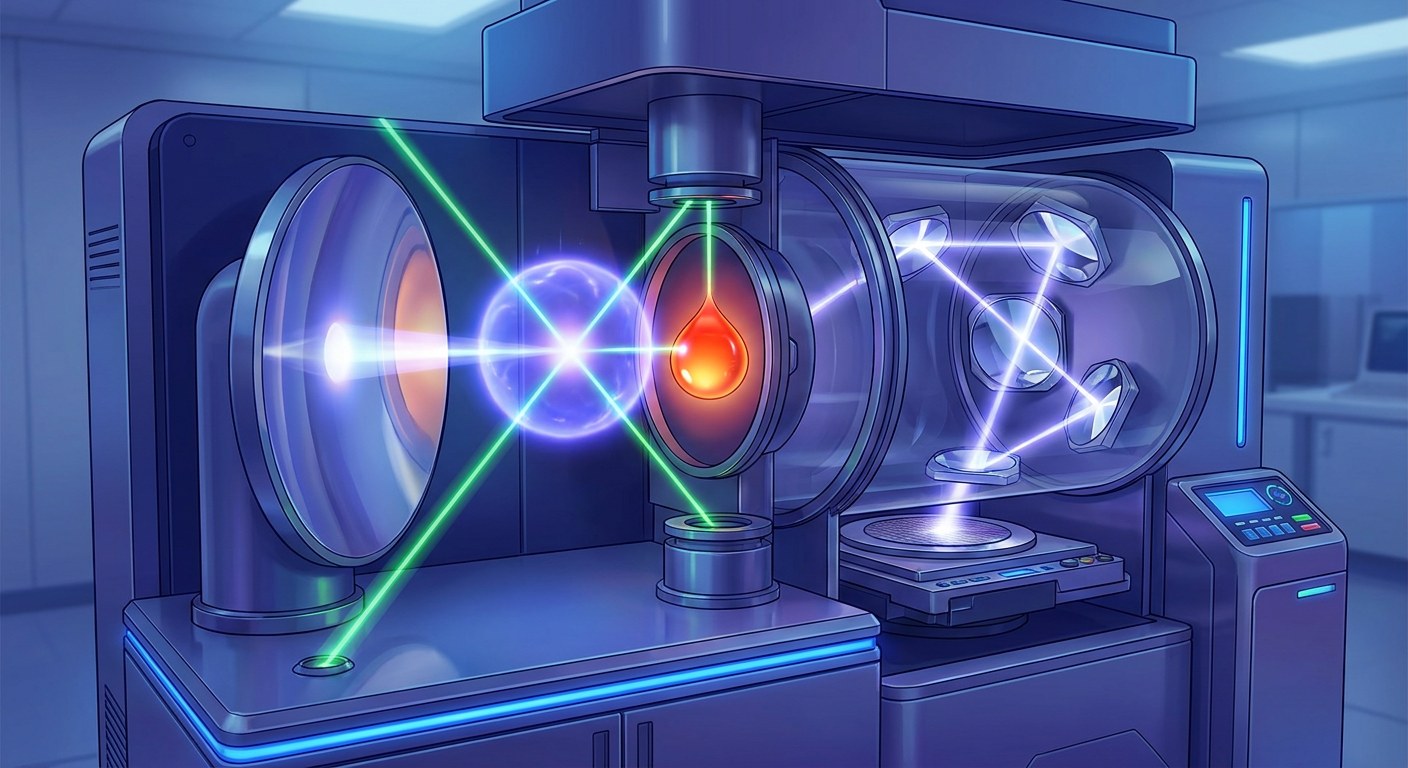
An EUV scanner is a catoptric system: all of its optics are mirrors, and the whole beam path runs in vacuum. The mirrors are not silver: they are stacks of forty to fifty alternating molybdenum and silicon bilayers, each a few nanometres thick, acting as a Bragg reflector. Constructive interference between the layers makes a mirror tuned for 13.5 nm reflect about 70 % of the light hitting it. That sounds like a lot until you count the path: between source and wafer the beam bounces off ten or eleven surfaces, including the mask. The result is that barely 1 % to 2 % of the generated light reaches the silicon. Which is why the most expensive chapter of the machine is precisely the source.
Fifty thousand tin droplets per second
The source is a laser-produced plasma (LPP) generator. An injector ejects droplets of molten tin about 25 micrometres across at 50,000 per second, travelling at some 70 metres per second. A first, weaker laser pulse hits the droplet and flattens it into a pancake; a second pulse, from a CO₂ laser of tens of kilowatts, arrives microseconds later and vaporises that disc. The tin becomes a plasma at tens of electronvolts — on the order of half a million kelvin, far hotter than the surface of the Sun — which emits strongly in the 13.5 nm band.
An elliptical collector mirror gathers that emission and concentrates it at the machine’s so-called intermediate focus, where the real available power is measured: current sources deliver on the order of 250 to 500 watts in that band. With an exposure dose of 20 to 30 millijoules per square centimetre, each wafer needs a few usable watts at the image plane and dozens of passes; which is why an EUV scanner runs at 150 to 220 wafers per hour and costs more than 200 million euros.
The mask is a mirror too
In classic photolithography the mask is a quartz plate with opaque areas: light passes through and projects its shadow. In EUV no transparency is possible, so the mask is a mirror with a pattern. The same molybdenum and silicon bilayers are deposited on a low-thermal-expansion glass substrate and, on top, an absorbing layer of tantalum and tantalum nitride (TaBN) is etched with the circuit pattern. Light strikes at an oblique angle — about six degrees — reflects off the unabsorbed areas, and the projection optics reduce it four times before it reaches the wafer.
That pattern is not the design as drawn. Because the absorber has real thickness, light behaves three-dimensionally as it reflects (mask 3D effects) and corners get rounded: the pattern etched into the mask carries optical proximity corrections (OPC) computed by electromagnetic simulation, with added shapes that look like blobs and compensate for what diffraction will distort.
Moving a wafer at half a metre per second without losing a nanometre
Projection is not a single shot photograph: the illuminated slit is a narrow strip and the system scans the wafer and the mask in sync, with the mask moving four times faster. The wafer travels at speeds on the order of half a metre per second, and the overlay error between layers must stay below two nanometres. To achieve that, the wafer stage floats on air bearings, is measured with laser interferometers and optical encoders, and disturbances are cancelled by voice-coil actuators in real time. The scanner carries twin stages: while one exposes, the other measures the height and alignment of the next wafer, so there are no pauses.
The final enemy: photon noise
With features a few nanometres wide, the number of photons hitting each point is small enough for their statistics to matter. This is stochastic noise: random dose variations that produce random defects, such as a line that breaks or two features that merge. Raising the dose reduces them but makes every wafer more expensive; shrinking the molecules of the photoresist also helps, at the cost of process stability.
The next generation, High-NA EUV, attacks the problem through the optics: it raises the numerical aperture from 0.33 to 0.55 with anamorphic mirrors, allowing features half the size to be printed without multi-patterning. The price is an exposure field halved, forcing each layer to be exposed in two passes and stitched together precisely, and a machine of some 150 tonnes already being installed at Intel and TSMC fabs. Lithography has stopped being applied optics and become a discipline of vacuum, plasmas and subnanometre metrology: the point where materials physics puts a ceiling on Moore’s law.