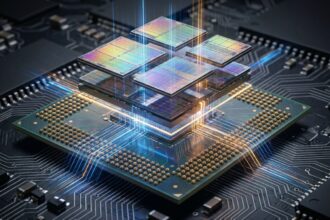

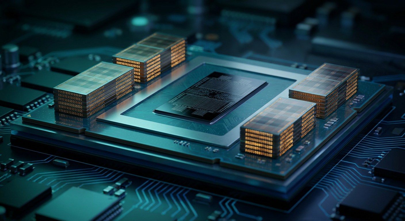
Look at the board of a modern graphics card through the right magnifier and you will not find a single piece of silicon next to the processor, but five or six smaller ones bonded to it. They are the HBM memory stacks, and each one is a skyscraper of eight or twelve floors of silicon pierced from top to bottom by thousands of vertical tunnels. That architecture, and not raw compute, is what decides today how many bytes per second an artificial intelligence chip can swallow.
A wall that has been growing for twenty years
Since the 1990s, a processor’s computing power has grown at close to three times every two years, while memory bandwidth has grown at 1.6 times. That asymmetry has a name in the industry: the memory wall. The practical consequence is that feeding those fast arithmetic units takes ever more data movement.
A concrete comparison helps. A DDR5 memory channel in a current computer, 64 bits wide and running at 6,400 million transfers per second, delivers about 51 GB/s. A single HBM3E stack, the generation used by 2025 cards, runs at roughly 1.2 TB/s: twenty-three times more, from a structure the size of a thumbnail. A GPU such as the B200 adds up to 8 TB/s across its eight stacks, and a server holding eight of those cards reaches 64 TB/s in aggregate.
The fix was not going faster, but wider and shorter
What makes HBM fast is not frequency but geometry. DDR memory connects over a 64-bit bus per channel, and raising throughput means raising the clock, which drives up power draw and interference. HBM does the opposite: it uses a 1,024-bit bus per stack, widened to 2,048 bits by the HBM4 standard, with 32 independent channels split into 64 pseudo-channels. By spreading the traffic over far more wires, each pin can run at a moderate rate, in the range of 6 to 8 Gbit/s, and the energy per bit collapses: between 3 and 4 picojoules per bit in HBM against 10 to 15 picojoules in DDR5. Across a data centre with thousands of accelerators, that gap is measured in megawatts.
The second trick is distance. Memory dies talk to each other through vias that run through the silicon from side to side (TSV, through-silicon via): cylinders about five micrometres across, spaced 40 to 50 micrometres apart, of which around ten thousand fit in a single die. A DDR5 module has roughly 1,300 pins in total; one HBM stack offers more than eight times as many signal paths, and each of them is far shorter: micrometres of silicon instead of centimetres of circuit board, and only tens of micrometres of material to cross. Less parasitic capacitance, less impedance, less energy per transition. Stacking does not make the wire shorter: it makes the wire almost disappear.
Underneath the stacks sits another unusual part. HBM is not soldered to the board but mounted on a silicon interposer: an oversized chip acting as a bridge between the compute die and the memory, able to exceed 2,500 square millimetres, one of the largest pieces of silicon ever manufactured. This is known as 2.5D integration: the chips are not stacked on top of each other but placed side by side on that bridge, joined by microscopic solder bumps. The complete package is called CoWoS, short for chip on wafer on substrate, and today it is one of the hardest bottlenecks in the whole manufacturing chain.
The bottleneck has a name: one token
All of this makes sense when you watch a language model answering. To generate each word, the machine has to read the model’s entire weight matrix from memory while performing barely two arithmetic operations per number read. The ratio of computation to data moved, the arithmetic intensity, stays near one FLOP per byte: three orders of magnitude below what a well-organised matrix multiplication achieves during training. The roofline model, which charts achievable throughput against arithmetic intensity, draws it as a slope: below a certain point, the curve is limited not by the cores but by memory.
The numbers are harsh. A model with 70 billion parameters at 16-bit precision occupies about 140 GB. If all of it must be read for every generated word, the minimum time per word is the model size divided by bandwidth: about 42 milliseconds on an H100 with 3.35 TB/s, and about 17 milliseconds on a B200 with 8 TB/s. No improvement in arithmetic units changes that equation. It is why the industry leans on quantisation, on batching many requests together, on speculative decoding and on reduced attention windows: all of them are ways of amortising the cost of reading memory. It is also why long-context attention, which additionally keeps a key-and-value cache that grows with the context, presses twice on capacity and bandwidth.
From standard to product: the HBM4 numbers
The current standard was approved in April 2025: JEDEC JESD270-4, known as HBM4. It defines a 2,048-bit bus per stack, twice the width of its predecessor, up to eight gigabits per pin and, with that, a nominal ceiling of two terabytes per second per stack. It supports 24 or 32 gigabit dies and stacks of 4, 8, 12 or 16 layers, which allows 64 GB in a single tower. Manufacturers do not stop at the paper spec: commercial parts already exceed it, with per-pin rates of 10 to nearly 12 Gbit/s that push each stack past three terabytes per second.
The deeper change in this generation is not just about numbers. In HBM3E the base die, the foundation of the tower that manages the interface, was DRAM made with the same recipe as the layers above it. In HBM4 that die becomes custom logic built on a different foundry process, opening the door for each customer to put its own functions inside the stack. The trend points to hybrid bonding, which does without solder bumps entirely, to cut the energy per bit even further.
What stacking costs
None of this is free. HBM costs three to five times more per gigabyte than DDR5, cannot be expanded later and halves the area available to the chip using it. It also dissipates heat where there is little margin left: memory dies must refresh themselves and slow down when they get hot, and squeezing them between layers of silicon makes cooling harder. On top of that, every stack goes through an expensive stacking and testing stage, with the risk of losing the whole assembly.
Even so, the wall does not vanish: it moves. Moving data between a chip and the memory in its own package is, more or less, solved. What comes next is moving it between chips, between cards and between racks, where copper is starting to fall short and where in-package optical interconnects are already being discussed. The next decade of artificial intelligence will be decided, once again, by data transport rather than by arithmetic.