
For forty years the rule was simple: a processor was a silicon wafer cut into dies, and each die held the whole system. That model is running out of road for two very physical reasons. The first is that the tool which draws the transistors, the extreme-ultraviolet scanner, can only expose a field of 26 by 33 millimetres: 858 square millimetres. That rectangle is called the reticle, and it is the largest a single die can be without stitching tricks that nobody uses in production today. The second is yield arithmetic: the more area, the higher the chance that a microscopic defect lands inside and ruins the whole circuit.
The sum that forced a change of strategy
The industry models that waste with a simple formula, the Poisson yield: Y = e−A·D₀, where A is the die area and D₀ the defect density per square centimetre of the process. At 0.1 defects per cm², a 100 mm² die comes out good 91 % of the time; a 600 mm² one, barely 55 %. A modern AI accelerator sits near 800 mm², the reticle ceiling: there yield collapses, and every 300-millimetre wafer — tens of thousands of dollars in a 3-nanometre node — delivers far fewer usable chips than its area would suggest.
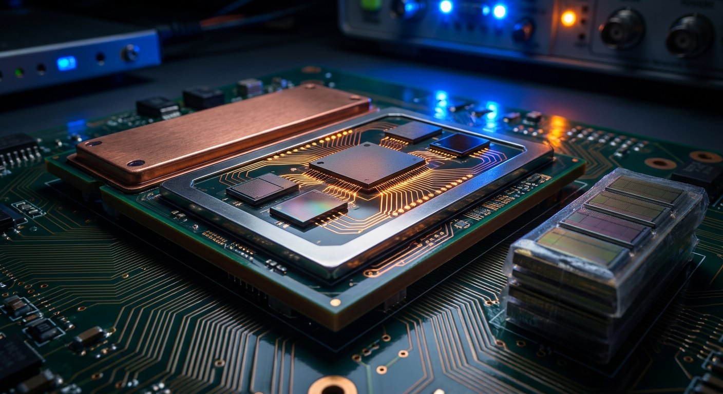
The answer is the chiplet: instead of one monolithic die, the product is split into several smaller pieces, each built in the node that suits it, tested separately and joined afterwards in a single package. If one compute piece comes out defective, that piece is scrapped, not the whole assembly; the ones that do work — the so-called known good die — go on to assembly. The saving is twofold: less silicon thrown away, and the option of building the input/output part, which gains nothing from smaller transistors, in a mature and much cheaper node.
What you already carry without knowing
AMD’s EPYC processors were the first big commercial deployment of the idea: several eight-core CCDs, roughly 80 mm² each, surround an I/O die of more than 400 mm² built in an older node. Apple joined two M dies through its own interface, UltraFusion, to double the cores without paying for a giant die. Intel called its version tiles and uses it in Meteor Lake laptops, where the compute, graphics, media and I/O dies are manufactured separately.
The catch is that those dies must talk to each other with bandwidth close to that of internal memory, and that is where the easy part ends. Conventional serial links, the SerDes used by PCIe or Ethernet, burn on the order of 5 picojoules per transmitted bit and add tens of nanoseconds of latency: fine for an expansion bus, not enough for two halves of a CPU to behave as one. The solution is a parallel, short, protocol-light link, with copper traces running from one die to the other through the substrate.
The standard that brought order: UCIe
For years every vendor invented its own interface — Infinity Fabric at AMD, EMIB and proprietary links at Intel — which tied customers to a single supplier. In March 2022 a consortium including Intel, AMD, Arm, Google, Meta, Microsoft, Qualcomm, Samsung and TSMC published UCIe (Universal Chiplet Interconnect Express), an open standard for that physical layer and its protocol. UCIe 1.0 defined two flavours: one for cheap packages, with bump pitch of 100 to 130 micrometres, and one for advanced packaging, with 45 and 25 micrometre pitches that allow thousands of contacts per millimetre of edge. The resulting density is measured in hundreds of gigabytes per second per millimetre of edge, with a power target below half a picojoule per bit — an order of magnitude better than a SerDes.
Version 2.0, in August 2024, added link management and diagnostics aimed at three-dimensional assembly; 3.0, already in 2025, raised per-lane speed and reach. The important detail is that UCIe does not force a packaging technique: it defines the physical layer and lets the integrator choose how to connect the dies.
Three ways to glue silicon together
The first is the silicon interposer: an extra wafer, with no active transistors but several metal layers, on which the dies are placed. It is the basis of TSMC’s CoWoS family and what brings HBM memory next to the processor with thousands of connections. Its limit is the old one, the reticle: the interposer is also exposed field by field, and current versions reach two or three times that size, with seams between fields that demand alignment accuracy below one micron.
The second is the organic substrate with redistribution layers, cheaper and with lower trace density: dies are connected through fine routing deposited on top of the substrate, with no silicon wafer needed. The third is local bridges: small silicon pieces embedded in the substrate that cover only the area where two dies meet, like Intel’s EMIB. They save interposer area and keep high density where it is needed.
Meanwhile, vertical connection has changed in nature. For years chips were stacked with tin microbumps and solder, at pitches of tens of micrometres. Hybrid bonding removes the solder: surfaces are polished flat at atomic scale, copper pads and dielectric are brought into contact, and an anneal at several hundred degrees makes the copper diffuse and bond. With 9-micrometre pitches already in production and roadmaps toward one or less, the density of vertical connections multiplies tenfold, and with it the bandwidth between a cache layer and its processor.
What hurts: heat, current and a mechanical war
Stacking and gluing solves performance but creates new problems. The first is thermal: an AI processor draws more than a thousand amps at under one volt, and that current must travel from the board to the die through substrate, interposer and thousands of microbumps. Every millivolt lost along the way is power turned into heat where there is no heatsink. That is why modern packages embed capacitors in the substrate and put voltage regulators ever closer to the silicon.
The second is mechanical. Silicon, copper and organic resin expand differently as they heat; in a 100 by 100 millimetre package that becomes warpage of tenths of a millimetre, enough to crack joints or lift layers. The third is testing: a loose die can be probed on the wafer, but a stack of eight memory layers can only be validated as a whole, and if it fails the entire assembly is scrapped.
The practical consequence is that chiplets are not free: they demand high volume to amortise the interposer design, placement tools with submicron precision, and a thermal and mechanical integration team that used to be unnecessary. In exchange, the industry has found something the monolithic die could no longer give it: keep growing when the reticle says enough. And the next frontier is already in the labs: bringing light, in the form of integrated optical links, to the very edge of the package.