
The smallest transistor manufactured at scale today is drawn with a light that cannot cross a single centimetre of air. That is not a metaphor: the photons tracing the interconnects of a 3-nanometre chip have a wavelength of 13.5 nanometres and are absorbed by any gas they meet, oxygen included. The whole machine that produces them —the extreme ultraviolet lithography scanner, EUV for short— runs in vacuum, uses mirrors instead of lenses, and fires at a target as improbable as a droplet of molten tin hit by a laser fifty thousand times per second.
Why the old light stopped working
For two decades the industry patterned chips with 193-nanometre argon fluoride lasers, immersing the wafer in ultrapure water to raise the refractive index and stretch the diffraction limit. The problem is mathematical: the resolution of an optical system is proportional to the wavelength divided by the numerical aperture. With 193 nm and an aperture of 1.35 you can separate features around 38 nanometres wide, and below that you must chain multiple exposures —multi-patterning—, each with its own cost, its time penalty and its accumulated misalignment risk.
The natural way out was shorter light, and that is where extreme ultraviolet sat waiting. But in that band there are no transmissive lenses: every material absorbs. Hence three consequences that define the entire architecture of the scanner: purely reflective optics, an optical path in vacuum, and a light source that has to be invented from scratch, because no laser emits directly at 13.5 nm with enough power.
The source: tin, two pulses and a plasma at 220,000 °C
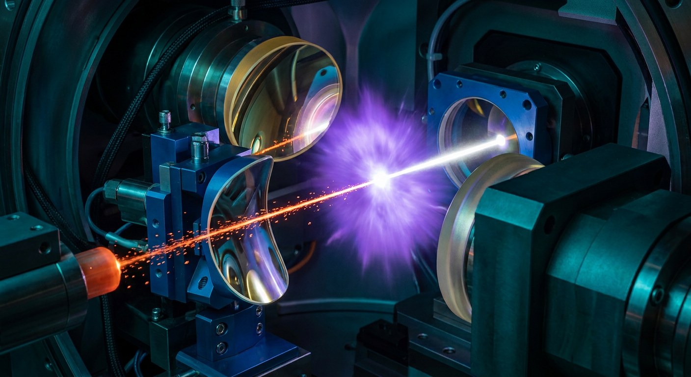
The source works like this. A generator produces tens of thousands of molten tin droplets per second, about 25 micrometres across, and hurls them towards the centre of the chamber. A first laser pulse, narrow and low-energy, strikes the droplet and flattens it into a sort of momentary pancake. A second, much wider and more powerful pulse —tens of kilowatts, generated by a CO2 laser running through a chain of amplifiers— hits that pancake and turns it into plasma at roughly 220,000 °C. That plasma radiates in every direction, including the 13.5 nm band.
The efficiency is brutally low: of every hundred units of laser energy that go in, about five come out as usable EUV. A collector mirror, with a hole in the middle for the pulses to pass through, gathers the light and sends it into the rest of the system. Everything else —heat, debris, vaporised tin— has to be managed so it does not contaminate the optics.
Mirrors that reflect by adding up phases
An ordinary metal-surface mirror reflects very little light at 13.5 nm. The scanners use Bragg reflectors: between forty and fifty alternating bilayers of molybdenum and silicon, deposited in vacuum with sub-nanometre precision and a total period of about 7 nanometres. The partial reflections from each interface emerge in phase and add up, so the stack reflects around 70 % of the incident light in the right band.
That 70 % looks good until you multiply it. The optical path includes the collector, the mask mirror, several projection mirrors and the mask itself: on the order of ten reflections. The result is that barely 1-2 % of the generated light reaches the wafer. That is why the source needs the power it needs, and why pushing the mask to the edge of its exposure capability is an exercise in optical patience.
The mask, the reduction and the impossible mechanics
The mask is reflective too: a surface with an absorber etched on top of it, struck by light at an angle. The projection optics reduce the image four times, so 100-nanometre details on the mask become 25 on the wafer. In the latest generation, the so-called High-NA, the numerical aperture rises from 0.33 to 0.55 and the optics become anamorphic: 8x reduction along one axis and 4x along the other, which forces the field to be exposed in two halves that must later be stitched with atomic precision.
Beneath all of it sits the mechanics. The wafer moves at about one metre per second, with accelerations greater than a fighter jet’s, and its position has to be known and corrected to better than a nanometre, because the allowable overlay error between layers is only a few nanometres. The scanners use two twin stages taking turns: one measures and aligns, the other exposes, then they swap roles. The assembly weighs around 180 tonnes, and a tiny vibration is enough to ruin a batch.
The details nobody mentions
- Scarce photons. At 13.5 nm the energy per photon is high, but the required dose (tens of millijoules per square centimetre) arrives in low counts. Shot noise appears: statistical variations that translate into stochastic defects, resists randomly under- or over-developed.
- Chemically amplified resists. A single photon triggers a chain reaction in the polymer. That is how sufficient sensitivity is achieved, and at the same time the source of blur and unwanted acid diffusion.
- The node is not a size. The marketing “3 nm” or “2 nm” does not correspond to any physical dimension of the chip: it is a commercial label inherited from the era when it did.
The result is one of the most concentrated supply chains on the planet. A single manufacturer sells EUV scanners, and inside each one the optics come from a single precision supplier and the laser from one particular photonics company. Behind every phone, tens of thousands of tin droplets are sacrificed each second so that a pattern of light lands where it should.