
In an artificial intelligence data centre there are cards that draw more than 700 watts, perform on the order of two thousand trillion floating-point operations per second and need liquid cooling to avoid melting. And even so they spend a good part of their time waiting. They are not waiting for the user or for the network: they are waiting for memory. Not because they lack space, but because the data takes too long to travel the path between where it is stored and where it is computed.
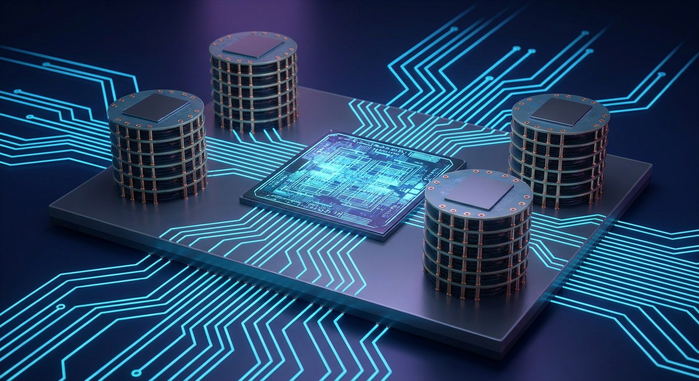
That path is measured in millimetres. Literally. In an ordinary computer, memory is a bank of chips sitting several centimetres away from the processor, joined by copper traces on a board. In an AI accelerator, the memory is glued next to the compute die, on a silicon substrate, and connected through microscopic copper pillars. That difference in scale, a few millimetres instead of a few centimetres, is today one of the variables that decides how much artificial intelligence a data centre can serve.
The memory wall
The gap goes back a long way. For four decades processors improved their computing power at a rate close to doubling every two years or less, adding cores, widening vector units and shrinking the lithography. Dynamic memory (DRAM), on the other hand, improved its bandwidth at a much slower pace, on the order of 30% a year, and its latency — the time it takes to return a requested piece of data — has been practically frozen since the 1990s: around 100 nanoseconds. One hundred nanoseconds in which a modern 4 GHz CPU could execute some 400 instructions. Hence the name this imbalance is known by: the memory wall.
Engineers model it with the so-called roofline: for each algorithm you compute its arithmetic intensity, that is, how many operations it performs for every byte it moves. If that number is low, performance depends not on the chip FLOPs but on the gigabytes per second it can swallow, and adding more compute units achieves nothing. A large language model, in the phase where it answers, sits on the worst side of that frontier.
Prefill and decode: why an answering AI is pure data movement
Running inference on a language model has two very different phases. The first, prefill, processes all the tokens of the message you send in one go: these are large matrix multiplications solved in parallel, and they saturate the compute units. The second, decode, generates the answer token by token, and there the pattern changes completely: to produce each token the machine must read every weight in the model. A 70-billion-parameter model at 16-bit precision occupies around 140 GB. Reading it entirely at the 4.8 TB/s an H200 delivers takes about 29 milliseconds, which sets a ceiling of roughly 34 words per second for a single user, whatever the chip FLOPs may be.
The way out of that ceiling is batching: if 32 users ask at the same time, the same 140 GB of weights is read once and reused for 32 tokens, so the card stops idling. The problem is the other half of memory, the half that grows with the conversation: the KV cache.
How much memory it takes not to forget what you have already been told
Every attention layer stores two tensors per token, the key and the value, holding the information the model needs in order to look back without recomputing everything. Round figures for a 70B model with 80 layers, 8 key/value heads and dimension 128: with an 8-bit cache you need 160 KiB per token, that is, some 21.5 GB for a 128,000-token conversation; at 16 bits it climbs to almost 43 GB. And that is per open conversation. If the model used classic multi-head attention, with 64 heads instead of 8, the bill per token would multiply by eight, up to 343 GB: a single user’s conversation would not fit on any card.
That is why modern architectures share the key and value heads (the trick called GQA), quantise the cache to 4 or 8 bits, page it in blocks so as not to over-reserve (paged attention) or push it to disk and bring it back when needed. All of that is software saving memory because memory is the scarce resource.
How to fit a 1024-bit channel inside one package
The hardware answer is called HBM, high-bandwidth memory. Instead of a module with a 64-bit bus, an HBM chip stacks 8 to 12 DRAM dies on top of one another and stitches them together with thousands of vias that pierce the silicon (TSVs). The result is a single component with an internal bus of 1024 bits per stack. An HBM3E at 9.6 Gbps per pin delivers about 1.23 TB/s; matching that with DDR5 modules at 51 GB/s would take some 24 sticks, each with its own socket and its own copper traces.
The reason the bus is widened instead of the frequency raised is physics, and it is a matter of energy. Moving one bit of information costs energy proportional to the capacitance of the wire, to the square of the voltage and to the switching frequency, and it grows with the length of the path. Travelling centimetres of board at high frequency costs on the order of 5 to 7 picojoules per bit; travelling millimetres through a silicon substrate, at half the voltage and with less capacitance, drops to half that or less. On a card moving tens of terabytes per second, that difference turns into hundreds of watts. Wide and slow beats narrow and fast.
Underneath the memory dies there is also a logic chip, the base die, which stores nothing: it acts as a gatekeeper. It handles the training and calibration of the vias, power distribution, error correction and the repair logic in case some column comes out defective from the factory. It also watches temperature, because DRAM loses electrons and needs refreshing, and above roughly 85 degrees the refresh rate doubles: exactly the opposite of what a hot chip wants.
The silicon bridge: interposers and direct bonding
Gluing the compute die and the memory stacks together requires a substrate that connects them with thousands of lines in a minimal space. That substrate is the interposer, a silicon wafer on which both are placed using solder microbumps 40 or 50 micrometres apart. This is the technique known as 2.5D, and its limit is that of lithography itself: one exposure field of the photolithography machine measures 26 by 33 millimetres, about 858 mm², and today’s interposers exceed that size by chaining several fields together, with the cost and the defects that implies.
The next step does without the interposer: instead of a complete silicon bridge, redistribution layers are laid on the organic substrate itself with small silicon bridges only where density is needed. And the final step is hybrid bonding, which welds copper against copper without solder balls, with pitches below 10 micrometres. There the distances drop to micrometres and the thermal path between dies improves, something critical when everyone wants memory to compute as well.
All of this is packaging, and packaging has become the industrial bottleneck. A single high-end package carries eight HBM stacks and two reticles of logic: if a single die is bad, the whole assembly is lost, so every one of them is tested before assembly (known good die), and the packaging production lines — CoWoS at TSMC, with its capacity booked years in advance — set how many accelerators the world can build each year.
What comes next: HBM4, memory that computes and light between chips
The next generation, HBM4, doubles the bus to 2048 bits per stack and raises it to 6.4-8 Gbps per pin, so each stack goes from 1.2 to about 2 TB/s and from 36 to 48 GB of capacity depending on how many dies are stacked. It also brings a structural change: the base die stops being a standard chip from the memory maker and becomes a custom design manufactured at the customer’s foundry. Memory stops being a component you buy off the shelf and becomes part of the accelerator design.
In parallel there are other routes around the same wall. Compute-in-memory puts arithmetic units inside the DRAM chip itself to add or accumulate without moving the data out. CXL uses PCIe to expand a server’s memory with external modules, albeit with higher latency. Cheaper inference accelerators rely on LPDDR, the memory used in phones, because they prioritise capacity and watts over raw bandwidth. And where copper no longer reaches, between and inside racks, optical links are appearing in an attempt to make packaging cost, rather than transistor cost, the thing that sets the limits.
What all this says about the coming years
The awkward conclusion is that the problem has long since stopped being solvable by adding gigabytes, because the scarce resource is not space but distance and energy per bit. Every real advance of recent years has consisted of shortening that path: gluing memory to the chip, piercing silicon vertically, eliminating solder, sharing weights between users. When you read a headline about the price of AI, it is worth remembering that a growing part of what is paid for is not computation, it is millimetres.